- 您现在的位置:买卖IC网 > Sheet目录2009 > MAX19506ETM+T (Maxim Integrated Products)IC ADC 8BIT 2CH 100MSPS 48TQFN
MAX19506
Dual-Channel, 8-Bit, 100Msps ADC
______________________________________________________________________________________
15
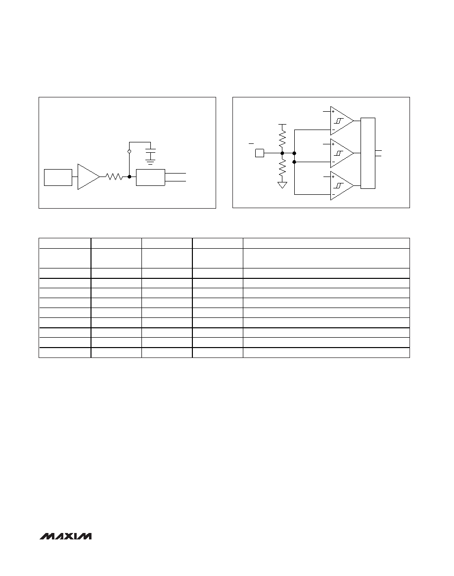
Reference Input/Output (REFIO)
REFIO adjusts the reference potential, which, in turn,
adjusts the full-scale range of the ADC. Figure 4 shows
a simplified schematic of the reference system. An
internal bandgap voltage generator provides an internal
reference voltage. The bandgap potential is buffered
and applied to REFIO through a 10k
resistor. Bypass
REFIO with a 0.1F capacitor to GND. The bandgap
voltage is applied to a scaling and level-shift circuit,
which creates internal reference potentials that estab-
lish the full-scale range of the ADC. Apply an external
voltage on REFIO to trim the ADC full scale. The allow-
able adjustment range is +5/-15%. The REFIO-to-ADC
gain transfer function is:
VFS = 1.5 x [VREFIO/1.25] Volts
Programming and Interface
There are two ways to control the MAX19506 operating
modes. Full feature selection is available using the SPI
interface, while the parallel interface offers a limited set
of commonly used features. The programming mode is
selected using the SPEN input. Drive SPEN low for SPI
interface; drive SPEN high for parallel interface.
Parallel Interface
The parallel interface offers a pin-programmable inter-
face with a limited feature set. Connect SPEN to AVDD
to enable the parallel interface. See Table 1 for pin
functionality; see Figure 5 for a simplified parallel-inter-
face input schematic.
BANDGAP
REFERENCE
BUFFER
1.250V
REFIO
INTERNAL GAIN—BYPASS REFIO
EXTERNAL GAIN CONTROL—DRIVE REFIO
SCALE AND
LEVEL SHIFT
INTERNAL REFERENCE
(CONTROLS ADC GAIN)
10k
0.1
F
EXTERNAL BYPASS
Figure 4. Simplified Reference Schematic
36k
156k
CS
SCLK
SDIN
AVDD
29/32 AVDD
DECODER
TO
CONTROL
LOGIC
23/32 AVDD
3/32 AVDD
Figure 5. Simplified Parallel-Interface Input Schematic
SPEN
SDIN/FORMAT
SCLK/DIV
CS/OUTSEL
DESCRIPTION
0
SDIN
SCLK
CS
SPI interface active. Features are programmed through the
serial port (see the Serial Programming Interface section).
1
0
X
Two’s complement
1
AVDD
X
Offset binary
1
Unconnected
X
Gray code
1
X
0
X
Clock divide-by-1
1
X
AVDD
X
Clock divide-by-2
1
X
Unconnected
X
Clock divide-by-4
1
X
0
CMOS (dual bus)
1
X
AVDD
MUX CMOS (channel A data bus)
1
X
Unconnected
MUX CMOS (channel B data bus)
Table 1. Parallel-Interface Pin Functionality
X = Don’t care.
发布紧急采购,3分钟左右您将得到回复。
相关PDF资料
MAX19515ETM+T
IC ADC 10BIT 2CH 65MSPS 48TQFN
MAX19516ETM+T
IC ADC 10BIT 2CH 100MSPS 48TQFN
MAX19700ETM+T
IC ANLG FRNT END 48-TQFN
MAX19705ETM+
IC ANLG FRNT END 48-TQFN
MAX19706ETM+T
IC ANLG FRNT END 48-TQFN
MAX19707ETM+T
IC ANLG FRNT END 48-TQFN
MAX19708ETM+
IC ANLG FRONT END 11MSPS 48-TQFN
MAX19710ETN+T
IC ANLG FRNT END 56-TQFN
相关代理商/技术参数
MAX19506EVKIT+
功能描述:数据转换 IC 开发工具 MAX19505-07/15-17 Eval Kit RoHS:否 制造商:Texas Instruments 产品:Demonstration Kits 类型:ADC 工具用于评估:ADS130E08 接口类型:SPI 工作电源电压:- 6 V to + 6 V
MAX19507ETM+
功能描述:模数转换器 - ADC 8-Bit 2Ch 130Msps 1.8V Precision ADC RoHS:否 制造商:Texas Instruments 通道数量:2 结构:Sigma-Delta 转换速率:125 SPs to 8 KSPs 分辨率:24 bit 输入类型:Differential 信噪比:107 dB 接口类型:SPI 工作电源电压:1.7 V to 3.6 V, 2.7 V to 5.25 V 最大工作温度:+ 85 C 安装风格:SMD/SMT 封装 / 箱体:VQFN-32
MAX19507ETM+T
功能描述:模数转换器 - ADC 8-Bit 2Ch 130Msps 1.8V Precision ADC RoHS:否 制造商:Texas Instruments 通道数量:2 结构:Sigma-Delta 转换速率:125 SPs to 8 KSPs 分辨率:24 bit 输入类型:Differential 信噪比:107 dB 接口类型:SPI 工作电源电压:1.7 V to 3.6 V, 2.7 V to 5.25 V 最大工作温度:+ 85 C 安装风格:SMD/SMT 封装 / 箱体:VQFN-32
MAX19507EVKIT+
功能描述:数据转换 IC 开发工具 MAX19505-07/15-17 Eval Kit RoHS:否 制造商:Texas Instruments 产品:Demonstration Kits 类型:ADC 工具用于评估:ADS130E08 接口类型:SPI 工作电源电压:- 6 V to + 6 V
MAX1950ETM
制造商:Rochester Electronics LLC 功能描述: 制造商:Maxim Integrated Products 功能描述:
MAX19515ETM/V+
功能描述:模数转换器 - ADC Dual-Channel 10-Bit 65Msps ADC RoHS:否 制造商:Texas Instruments 通道数量:2 结构:Sigma-Delta 转换速率:125 SPs to 8 KSPs 分辨率:24 bit 输入类型:Differential 信噪比:107 dB 接口类型:SPI 工作电源电压:1.7 V to 3.6 V, 2.7 V to 5.25 V 最大工作温度:+ 85 C 安装风格:SMD/SMT 封装 / 箱体:VQFN-32
MAX19515ETM/V+T
功能描述:模数转换器 - ADC Dual-Channel 10-Bit 65Msps ADC RoHS:否 制造商:Texas Instruments 通道数量:2 结构:Sigma-Delta 转换速率:125 SPs to 8 KSPs 分辨率:24 bit 输入类型:Differential 信噪比:107 dB 接口类型:SPI 工作电源电压:1.7 V to 3.6 V, 2.7 V to 5.25 V 最大工作温度:+ 85 C 安装风格:SMD/SMT 封装 / 箱体:VQFN-32
MAX19515ETM+
功能描述:模数转换器 - ADC 10-Bit 2Ch 65Msps 1.8V Precision ADC RoHS:否 制造商:Texas Instruments 通道数量:2 结构:Sigma-Delta 转换速率:125 SPs to 8 KSPs 分辨率:24 bit 输入类型:Differential 信噪比:107 dB 接口类型:SPI 工作电源电压:1.7 V to 3.6 V, 2.7 V to 5.25 V 最大工作温度:+ 85 C 安装风格:SMD/SMT 封装 / 箱体:VQFN-32